PCI Express, abbreviated as PCIe, is the first generation of the PCI Express expansion bus standard. It uses for connecting high-speed components within a computer system. The PCIe 1.0 specification was first introduced in 2002 and finalized in 2003 as a replacement for older PCI, PCI-X, and AGP standards. It provides significantly higher performance, scalability, and flexibility compared to its predecessors.
Key Features
Here are some key features involve in it:
- Serial Interface: PCIe is based on point-to-point serial links rather than a shared parallel bus architecture. This allows for higher clock speeds unconstrained by bus timing issues.
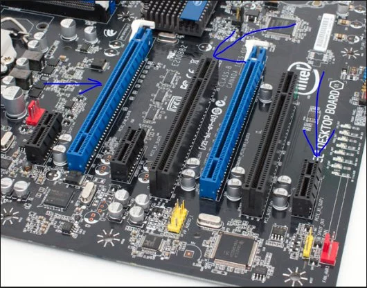
- Lane Based: PCIe connections consist of one or more serial lanes. Each lane provides a duplex connection with transmit and receive pairs. Common configurations are x1, x4, x8 and x16.
- Packet-Based: All information is encapsulated into packets for transmission across the serial link. Packets contain addresses, data, control symbols, and error detection codes.
- Higher Bandwidth: PCIe 1.0 provides up to 2.5 Gbit/s raw bandwidth per lane, per direction. An x16 slot has a total peak bandwidth of 32 Gbit/s.
- Hot Swap Support: Devices can be added and removed without impacting the system, enabled using special pins.
- Software Compatible: Existing PCI software can operate over PCIe through legacy compatibility features.
- PCIe Compatibility with 4.0 Slot: PCIe 1.0 cards are backward compatible and will work in PCIe 4.0 slots. The card will simply run at PCIe 1.0 speeds.
- Speed: PCIe 1.0 x1 slot provides 250MB/s in each direction, which is faster than a SATA 1.0 interface that provides up to 150MB/s total bandwidth.
Architecture
The PCIe system consists of a root complex and multiple endpoints connected via a switch. The root complex originates the PCIe hierarchy domain from the PCI Host bridge located on the motherboard.
It allows interaction between CPU, memory, and endpoints through logical lanes. Endpoints contain PCIe interfaces and can be peripheral devices or expansion slots. Switches allow multiple endpoints to connect to the root complex.
PCIe 1.0 Transaction Layer
The Transaction Layer is the middle layer in the PCI Express protocol stack. It handles the assembly and disassembly of data and commands into PCIe transaction layer packets (TLPs). It manages flow control, handles basic PCIe protocols, and ensures reliable delivery of packets.
Role of the Transaction Layer
The transaction layer sits in the middle of the PCIe protocol stack, between the logical PCIe device interfaces and the data link layer. It is responsible for reliably handling the communication of all PCIe information over the physical serial connection.
Key Responsibilities
- In the Packet Assembly process, it takes requests from the host, segments into TLPs, and assigns required headers for routing.
- Flow Control implements a credit-based system to manage TLP transmission and reception.
- Sequencing ensures the order of TLPs is maintained using sequence numbers.
- Retry Control manages TLP retries in case of errors or buffer overflows.
- Acknowledgments send ACK and NAK signals for successful and failed transmissions.
- Cyclic Redundancy Check (CRC) performs error detection on TLPs using the CRC field.
- Link Maintenance performs link training, width, and frequency negotiation.
- Power Management handles the transition of links between active and low-power states.
By handling these essential functions, the transaction layer establishes the foundation for seamless and reliable data transfer in PCIe communication.
TLP Types
The transaction layer defines a number of different TLP formats used to encapsulate various types of PCIe information:
- Memory Read/Write TLPs to access memory spaces.
- I/O Read/Write TLPs to access I/O mapped spaces.
- Configuration Read/Write TLPs to configure devices.
- Message TLPs for sideband signaling outside the normal flow.
- Completion TLPs to communicate transaction status.
Each TLP format contains the necessary fields like headers, packet sequence numbers, CRC values, acknowledgments, and data payloads.
PCIe 1.0 transaction layer handles the fundamental mechanics of transmitting PCIe protocol information reliably across high-speed serial links. By managing TLPs effectively, it enabled PCI Express to deliver huge leaps in performance compared to older standards.
PCIe 1.0 Data Link Layer
The Data Link Layer is the lowest layer in the PCI Express protocol stack. It acts as an interface between the transaction layer and the physical layer of the connection. Its main responsibilities are data encoding, link management, and error detection.
Key Responsibilities
- The data Encoding process involves encoding and decoding data using an 8b/10b encoding scheme before transmission over the physical layer.
- Link Management Manages the operation of single or multiple PCIe lanes. Handles lane reversal, scrambling, alignment, etc.
- Error Detection performs CRC checks and retry handling for transmission errors.
- Flow Control Initialization exchanges flow control credits and buffer allocation during link initialization.
- Sequence Numbering assigns sequence numbers and recovers the order of packets.
- Power Management handles the transition of links into low-power states for power saving.
By taking care of these crucial jobs, the data link layer enables the physical transmission of transaction layer packets reliably across PCIe links.
Encoding Scheme
A central aspect of the data link layer is the 8b/10b encoding, which converts 8-bit symbols into 10-bit symbols before transmission. Some key benefits of 8b/10b encoding are:
- Clock recovery from the data stream avoids a separate clock channel.
- DC-balanced symbols prevent baseline wander.
- Disparity allows for transmission error detection.
- Special symbols for link management and delimiters.
Physical Interface
At the physical layer, the PCIe connection consists of transmit and receive differential pairs called lanes. Data flows in both directions allowing full-duplex communication. The data link layer also handles hotplug events and lane reversal.
- Tx and Rx Lane Pairs: Serial differential pairs in each direction for full duplex transfer.
- Lane Reversal: Lanes can reverse direction dynamically for balancing.
- Hot Plug Support: Allows link reconfiguration during insertion or removal of devices.
PCIe 1.0 data link layer implements vital encoding, error detection, link management, and physical interface capabilities that ultimately allow PCIe devices to communicate reliably at gigabit speeds.
PCIe 1.0 Physical Layer
The Physical Layer is responsible for the electrical signaling and interfaces that enable the transmission of raw binary data across PCI Express links. It is the foundation on which high-speed PCIe communication is built.
Signaling Interface
Some key attributes of the PCIe 1.0 physical layer signaling:
- Differential signaling is used over simplex copper traces within the PCB to carry data. This allows for high noise immunity.
- Transmit and receive differential pairs act as lanes for individual data flow directions allowing full duplex transfer.
- Data is transmitted as low-voltage smooth analog waveforms rather than trapezoidal signals. This reduces electromagnetic interference.
- Techniques like 8b/10b encoding, lane spacing, and scrambling help minimize crosstalk interference.
- Additional sideband signals are used for functions like device reset and wake events.
Electrical Specifications
The PCIe 1.0 physical layer defines electrical parameters such as:
- 800-1600mV differential signal amplitude per lane.
- 2.5 Gbit/s bit rate per lane, scaling to 32 Gbit/s for an x16 slot.
- +/- 300 ppm per lane frequency tolerance for robust clock recovery.
- 165-1465mV differential input voltage range for the receivers.
Connectors and Cables
A variety of connector and cable options are defined for PCIe 1.0:
- The edge connector provides backward compatibility with PCI.
- Low-profile connectors allow smaller form factors.
- Internal board-to-board connectors.
- Support for copper cabling as well as optical connections.
PCIe 1.0 physical layer defines the signaling, electrical, and interface specifications necessary for high-speed serial transmission over the PCI Express protocol. It enabled PCIe adoption across diverse platforms and form factors.
PCIe 1.0 Power Management
PCI Express 1.0 introduced a new high-speed serial interface architecture for computer expansion slots and devices. This brought major improvements in performance, scalability, flexibility, and backward compatibility compared to legacy parallel buses.
Type 0 and Type 1 refer to the power delivery specifications for PCIe slots. Type 0 slots deliver up to 25W while Type 1 slots can deliver up to 75W to the card.
Topology
Some key aspects of the PCIe 1.0 system topology:
- The root complex located in the chipset originates the PCIe domain and provides physical PCIe lanes.
- Endpoints such as add-in cards and onboard devices connect to the root complex via a tree-like hierarchy.
- Switches enable multiple endpoints to connect to the root complex by forwarding packets between them.
- Lanes from the root complex are distributed among slots using switches. Wider slots get more lanes.
Hot-Plug Support
PCIe supports hot plugging of endpoints without impacting the system:
- Special pins detect card insertion and removal events.
- The data link layer handles the reconfiguration of links during hot-plugging.
- This provides easy device expansion and replacement.
Backward Compatibility
To ease adoption, PCIe 1.0 offers software compatibility with legacy PCI:
- Endpoints can emulate a PCI controller for seamless integration.
- Both logical and physical compatibility modes are defined.
Multi-GPU Support
The PCIe architecture facilitated multi-GPU systems for high-end graphics:
- Peer-to-peer lanes enable direct communication between GPUs.
- The hierarchical topology allows multiple GPU endpoints.
PCIe 1.0 established a robust and scalable high-speed serial architecture with excellent performance, flexibility, and backward compatibility for computer expansion.
PCIe 1.0 Performance
PCI Express 1.0 represented a monumental leap in I/O performance, bandwidth, and efficiency compared to legacy PCI. It enabled new levels of speed for graphics, networking, storage, and more.
Bandwidth
- Up to 2.5 Gbit/s raw bandwidth per lane and direction.
- x1 slot has 2.5 Gbit/s peak bandwidth.
- x16 slot has 32 Gbit/s total peak bandwidth.
- Over 4X increase compared to PCI-X 266 MHz.
- Bandwidth scales linearly with lane count.
Latency
- Very low latency overhead for transferring data.
- The high-speed serial interface has minimal interference.
- No bus arbitration delays like parallel PCI.
- Typical latency is around 35ns for data packets.
Efficiency
- Excellent efficiency even for small data transfers.
- No long bus turnaround penalties.
- Low latency results in high throughput.
- Low CPU overhead frees up host resources.
Scalability
- Performance scales seamlessly with wider links.
- No bandwidth-sharing tradeoffs like PCI.
- Easy performance upgrade from x1 to x2, x4, etc.
Summary
PCIe 1.0 enabled order-of-magnitude improvements in transfer bandwidth, latency, and efficiency over older standards. This allowed PCIe to meet the needs of high-bandwidth devices and demanding workloads.

About Author
I’m Zeshan, a passionate PC builder and gamer with a vision to empower fellow gaming enthusiasts with the best gaming gadgets available in the market. With over seven years of hands-on experience in the gaming industry, I’ve dedicated my life to exploring, testing, and reviewing cutting-edge gaming gear that takes your gaming experience to the next level.